2
\$\begingroup\$

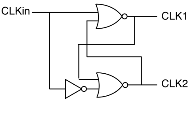
I have to use combinational logic to write Verilog for a circuit schematic. However, my output registers, CLK1 and CLK2, do not change and are stuck at the initial values. What is causing this bug? Here is the code and output:

//Verilog HDL for "HW8", "ClockCircuit" "functional" `resetall `celldefine `delay_mode_path `timescale 1ns / 10ps module ClockCircuit ( input wire CLKin, output reg CLK1, output reg CLK2 ); initial begin CLK1 = 0; CLK2 = 0; end // Intermediate signals wire inv_output; wire nor1_output; wire nor2_output; // Instantiate the inverter inv_1 inv ( CLKin, inv_output ); // Instantiate the first NOR gate nor_2 nor16 ( CLKin, nor2_output, nor1_output ); // Instantiate the second NOR gate nor_2 nor2 ( nor1_output, inv_output, nor2_output ); // Drive the outputs using procedural blocks always @(posedge CLKin) begin CLK1 <= nor1_output; CLK2 <= nor2_output; end endmodule `endcelldefine 

enter image description here

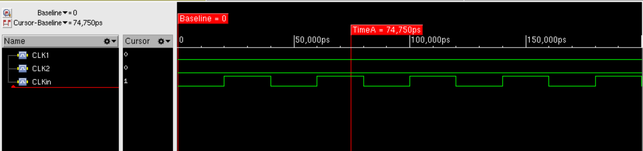
The circuit I'm trying to create is here:

enter image description here

\$\endgroup\$
1
  • \$\begingroup\$ Are you aware that the shown circuit does not store anything? CLK1 is always the inversion of CLKin, and CLK2 follows CLKin directly. \$\endgroup\$ Commented Dec 8 at 9:20

2 Answers 2

0
\$\begingroup\$

What is causing this bug?

You have a Verilog simulation race condition. All the signals in your code change at the same time, which means the output signals may not display all the actual transitions in your waveform viewer.

You need to change your Verilog code to use good coding style to avoid race conditions. For example, your schematic shows combinational feedback paths: CLK1 is fed back into logic driving CLK2, and vice versa. This looks like you are attempting to model some type of latch. It is improper to model latch behavior with gate-level modeling; you should use behavioral modeling instead.

\$\endgroup\$
0
\$\begingroup\$

Your Verilog and the desired circuit drawn are inconsistent. Take a look at the always @(posedge clkin) construct: this implies a pair of D latches clocked off the clkin signal at the output of your circuit.

Because the two NOR gates are going to be switching around the same time as clkin changes state, but always doing the same simulated thing at the same time, the output will remain stable in simulation. In reality not necessarily so.

I am pretty sure your simulator is not handling this 100% properly either, as at the instant 'clkin' changes state from 0 to 1 I would expect NOR1 output to be high and NOR2 output to be low.

Or maybe it does not implement the time-delta concept where all gates have a tiny propagation delay in simulation.

\$\endgroup\$

Start asking to get answers

Find the answer to your question by asking.

Ask question

Explore related questions

See similar questions with these tags.